

@suninhouse in terms of caches the fundamental element of memory is a bistable circuit that consists of two NAND gates that can hold a bit. On a slightly higher level, memory is a collection of transistors - for example SRAM units consists of 6 transistors while DRAM units consist of 1 transistor

@suninhouse As for the human part, I am not sure if brain has L1, L2 cache, but there is indeed a difference in short-term memory and long-term memory for our brain, whereas short-term memory is often brief and limited, which is sort of like the cache.

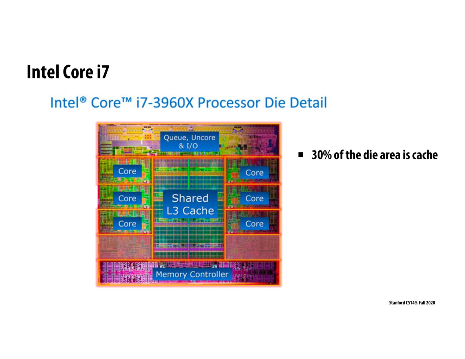
Why was the design choice made so that L3 cache is shared and not per-core like the other cache levels? Wouldn't it be more beneficial to communication overhead if this were not the case?

How do hardware/electrical engineers decide how to physically design a processor? Are there factors that are more/less important than we'd intuitively think?

I don't know if it's a matter of performance/efficiency in communication or ease of design, but I find it interesting that processors almost always seem to have clean looking layout with rectangular elements

I'm a little confused at the processor die image. I found a blown-up version here on WikiChip. Notably, there is a row right above the Memory Controller that doesn't have any labels. If you look closely, this row looks almost indistinguishable from the 3 right above it. I can't imagine that their function would be totally different! Doesn't the processor die suggest that the Intel Core i7-3960X is an octocore processor as opposed to a hexacore processor?
.png)
@kevtan yes I believe it’s probably the same die. From my understanding, it’s cheaper to share a die between different processor models, so that a lower end model with less cores can be obtained by physically disabling some of the cores. This is nice because manufacturers can then disable defective cores and still sell the processor
@msere Oh wow, that's cool! So that means cheaper processor models actually took the same amount of money to produce as more expensive processor models (in some cases)? And would that mean that it would be possible to take your processor and "unlock" some of the cores on the die?
@kevtan Yup that has been possible for some processors by flashing the firmware, if you were lucky enough to get a chip that had disabled cores that weren’t also defective. Most of the time though, the cores are physically destroyed to make this impossible. This is also possible on some to do on some older AMD GPUs, where you could unlock more cores. Based on this class I’m assuming that some models had disabled SMs, or whatever the AMD equivalent is called

Usually chips have a regular layout because the process of making the chip needs to be uniform, for example if one area is very dense and one area very sparse then when you try to make the chip it will cause difficulty for example for lithography since one requires small wavelength and dose and one requires large wavelength and different dose. Also it can cause thermal hotspots on the chip.
Please log in to leave a comment.
What are the physical foundations of different types of memories? By the way, just out of curiosity, how are these memories compared with human memory? Do we also have L1, L2, L3, cache? :-)