

In the limit, does this mean we'd have many different architectures, CPUs, GPUs, etc. on one giant chip with hardware logic to schedule jobs between them?

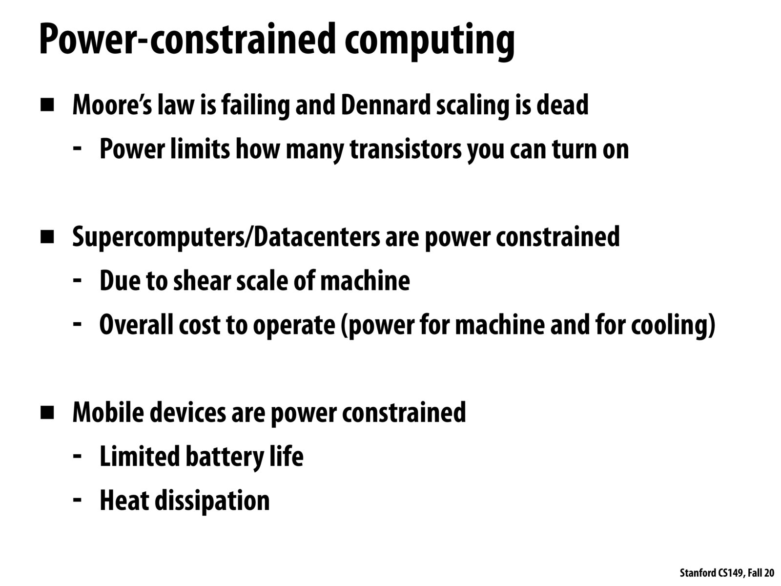
The power limit refers to the fact that if all the transistors within a chip are turned on, the power consumption will be huge and the heat dissipation simply cannot keep up. The part of the chip that cannot be turned on due to TDP limit is often referred to as "dark silicon".

What is the primary way chip designers manage to reduce the size of transistors (and thus put more transistors on the chip) nowadays? Are advances only hardware based or is there a software component? In reference to @teapot's comment, is the "dark silicon" of a chip determined dynamically, meaning that with additional or better cooling we could reduce the size of this inactive area?

@lfu My impression is that dark silicon is definitionally dynamic, including cooling and workload. Otherwise, if it is known that it can't turn on at manufacture time, why have circuitry on this area at all?
Please log in to leave a comment.
To support the first bullet point: the newest Intel fabrication plant, meant to build chips with minimum feature sizes of 10 nanometers was much delayed. Actually, it is delivered 5 years after the previous generation of chips with 14-nanometer features in 2019.